
Silicone Devices
The VLAIO innovation mandate aims to further develop our Silicone Devices proof-of-concept (lab-scale) fabrication process for disruptive new, soft electronic circuits into a sheet-to-sheet process with proven reliability for industry. This production process then serves as the cornerstone for a technology enabler spin-off.


Gallium based Liquid Metal Alloys (GaLMA’s), which are liquid at room temperature, present themselves as a key component for the domain of soft electronic circuits. GaLMA’s combine the inherently excellent conductivity of metals (just 1 order of magnitude below that of bulk silver and copper) with the inherent deformability of liquids. In addition, these materials are non-toxic, easy to apply to a broad variety of materials (high wettability) and stable in their patterned form.
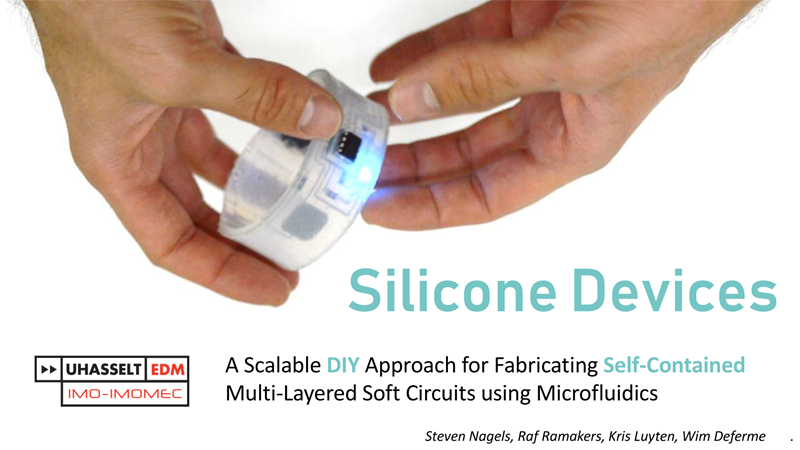
With the paper ‘Silicone Devices’ a fabrication process was presented which stands out in its combination of simplicity and performance. It poses as a research tool for everyone wanting to explore the possibilities of completely soft and stretchable electronic circuits. The focus was therefor put on using highly accessible materials and processing techniques. This work came together through collaboration of Raf Ramakers (EDM), Kris Luyten (EDM), Wim Deferme (imo-imomec) and Steven Nagels (imo-imomec) at Hasselt University, Belgium. The technique presented in this instructable is published at the premier venue in human-computer interaction: Human Factors in Computing Systems (CHI 2018).
In its current form, the Silicone Devices approach is able to convert a circuit design of arbitrary complexity from traditional PCB implementation to a realization in soft materials. Most research efforts constrain themselves to depositing GaLMA’s without integrating functional components in the soft circuit. With Silicone Devices, Commercial Off The Shelf (COTS) components are directly embedded inside the soft silicone matrix and manifest themselves as the only rigid elements. A way of chemically bonding these COTS components to the silicone matrix was illustrated by the authors. Circuits which do not use this bonding step, suffer from delamination between component and silicone matrix. This delamination allows for the GaLMA to flow around the component’s body and thus causes short circuits. GaLMA traces can furthermore run across multiple layers from one component to the other (multi layer) by incorporating VIA’s. All precision steps are executed by a computer controlled laser cutter: marking positions, patterning circuit traces, cutting VIA’s and cutting circuit outlines. The remaining steps are performed manually.
There is more in-depth information to read about Silicone Devices, if you’d like: here is the project page of the PhD work on Silicone Devices, the full academic publication can be found here, and a more general background on fabrication of interconnect based stretchable electronics can be found here.
The VLAIO innovation mandate aims to further develop our Silicone Devices proof-of-concept (lab-scale) fabrication process for disruptive new, soft electronic circuits into a sheet-to-sheet process with proven reliability for industry. This production process then serves as the cornerstone for a technology enabler spin-off which commits itself to bring a new generation of highly conformable electronic devices to market through a B2B approach of development and production with Flemish companies.
Contact
dr. ing. Steven Nagels

dr. Lieve De Doncker
