MAESTRO
MAESTRO proposes to develop solid-state qubit architectures for working at reasonably low or ambient conditions, as a compelling path towards industrially interesting medium scale quantum systems. The central aim of the proposal is to tackle the bottle neck issues of our technology for diamond processor hardware scalability, e.g., the deterministic engineering and fabrication of NV qubits with a high fabrication yield that will allow then to scale our technology to industrially relevant processes. MAESTRO will provide a quantum processor platform that can be further developed, in future, towards marketable industrial applications.


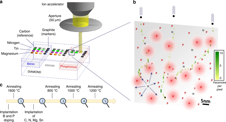
a Diamond sample with intrinsic, p-type and n-type areas (by implantation with [P] and [B]), and implanted additionally with carbon (as a reference) and nitrogen, tin, and magnesium to produce, NV, SnV and MgV centres b Illustration of the sample status after implantation c Time sequence of the different steps of the study. The magnifiers symbolise imaging spectroscopy
Aims:
(i) Optimisation of material technologies
(ii) Deterministic NV formation
(iii) Electrical readout of spin states
(iv) Device fabrication
WP1: Qubit fabrication
WP2: Device fabrication
WP3: Qubit control
WP4: Technology demonstrator
and use case analysis
Recent results, established within this consortium, established the possibility of near-deterministic generation of solid-state-qubits, NV centres in diamond. Placing them at a distance of about 10-40 nm would allow for high-fidelity two-qubit gates based on magnetic dipole-dipole coupling. The method of electrical readout of the spin, also discovered recently by consortium members, allows for individual spin qubit readout, dealing with the major constrain of the diamond quantum hardware scalability. At the same time we explore novel diamond colour centres that can operate as effective spin qubits.
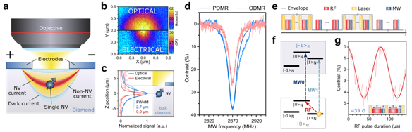
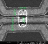
a Schematics for photoelectric readout of a single nuclear spin coupled to an electron spin. b Comparison between NV photoelectric and optical mapping. c High 2-photon ionisation depth resolution compared to optical resolution. d High spin contrast achieved for NV electron spin photoelectric detection. e, f, g 14N nuclear spin driving and photoelectric readout via entanglement to NV electron spin4, h nanolithography engineered contacts on diamond serving for electrical spin readout.
Partners


Contact
prof. dr. Milos Nesladek

dr. Lieve De Doncker
